Beyond Fine Pitch.
The Future of Wafer Probing
with 3D Printing
Moore's Law is under threat unless wafer probing evolves.
Shrinking component sizes and increased interconnect density needs dramatic innovation in probing technology to access finer pitch.
The limit of so-called "fine pitch" has long been reached, and for 10+ years there has been little progress in enabling testing smaller than 40 µm pitch.
What's the solution?

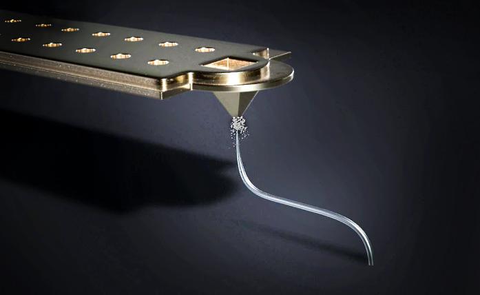
Innovation is Required to Reach Smaller Pitch
Current methods are not able to match the demand from industry, and chip designers have long had to compromise with DfT (design for test) considerations.
The lack of flexibility in probe design, probe pitch, and space transformer availability are all bottlenecks to continued scaling. In the face of increasingly complex wafer packaging solutions, probe testing needs to innovate.
Access <20 µm Pitch with 3D Printing
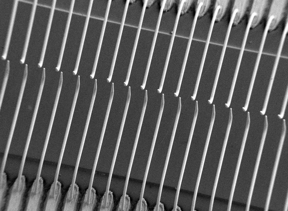
Unprecedented Possibilities
An SEM image of 3D printed probes with an alternating 18.5 µm / 35.5 µm pitch
Innovation for Continued Scaling
See how Exaddon's probe printing is changing chip design and probe testing
3D Printing: Unparalleled Possibilities in Customization, Pitch, & Lead Time
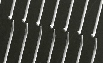
Beyond Fine Pitch
Contact pads and bumps at
less than 20 µm pitch
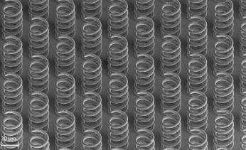
Endless Customization
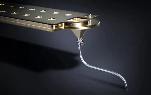
Template-free 3D printing for
amazing design freedom
Low Lead Time
Iterate designs fast;
maximize uptime & yield
How Does it Work?
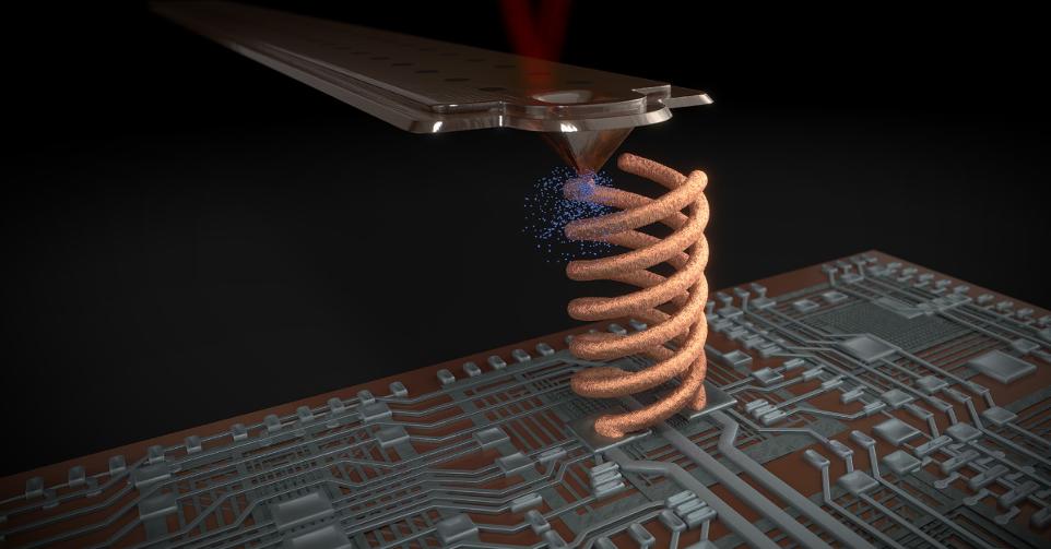
Printed material is mechanically stable with excellent conductivity and tensile strength. Read about the material properties here.